The TS9001 TDR System provides semiconductor manufacturers with flexible solutions for addressing a variety of failure analysis requirements. By establishing a low-cost failure analysis environment and enabling connections to high-frequency probing systems already in use by customers. TS9001 offers customers one of the shortest measurement times on the market.
Advantest’s leading-edge semiconductor test technology, and terahertz failure analysis technology supports the development of innovative semiconductor supply chains, while enhancing the customers’ quality control.
Background
As semiconductor packages (hereafter, devices) grow smaller and more highly integrated, the ability to locate failures with non-destructive, high-resolution technology is increasing in importance. Providing access to the industry’s most advanced failure analysis environment is critical to being able to address the wide variety of failure analysis issues that present in these complex devices. To meet these requirements, Advantest developed the TS9001 TDR System, which enables customers to direct-connect their high-frequency probing systems, to realize high-speed, high-resolution measurement.
Key Features
- High-speed and high-resolution measurement
The TS9001 TDR system, which utilizes an ultra-short pulse signal processing technology, achieves higher distance-to-fault resolution of 5 μm and precise fault location identification with the industry’s fastest class measurement time of 30 sec (Number of integration: 1024, 1/10 shorter than our conventional products). This is the same proven technology used in our ground-breaking terahertz analysis systems.
- Versatile connectivity for high-frequency probing systems
TS9001 can be configured with a high-frequency probing system owned or selected by the customer. It offers flexible solutions according to the device forms or fault analysis environments.
(1) Failure analysis of devices with micro bump
By connecting the TS9001 to a high-frequency probing system along with a high-resolution microscope, failure analysis of devices with micro bump of minimum diameter 50 μm is possible.
(2) Temperature control function
Failure analysis of devices kept in low/high temperatures is also possible, if the system is connected to a high-frequency probing system with a thermal-system function.
(*) TDR (Time Domain Reflectometry) is widely used to locate circuit failures. Input pulsed signals are reflected at circuit faults inside the device. Time domain analysis of the reflected waveform allows users to determine the fault location and failure mode (open or short) by waveform comparison between good device and failed device. The peaks appeared only in the failed device are analyzed, to identify them.
Key Specifications:
Fault position locating resolution: 5 μm
Maximum measurement length: 100 mm
Measurement time: 30 sec (Number of integrations: 1024, Probe contact time not included)
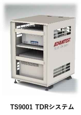
Size/Weight: 600 mm (W) x 700 mm (D) x 860 mm (H)/100 kg or less
For more information on this system, visit our Website.
URL: https://www.advantest.com/products/terahertz-spectroscopic-imaging-systems/tdr-option
Advantest (TSE: 6857) is the leading manufacturer of automatic test and measurement equipment used in the design and production of semiconductors for applications including 5G communications, the Internet of Things (IoT), autonomous vehicles, artificial intelligence (AI), machine learning, smart medical devices and more. Its leading-edge systems and products are integrated into the most advanced semiconductor production lines in the world. The company also conducts R&D to address emerging testing challenges applications, produces multi-vision metrology scanning electron microscopes essential to photomask manufacturing, and offers groundbreaking 3D imaging and analysis tools. Founded in Tokyo in 1954, Advantest is a global company with facilities around the world and an international commitment to sustainable practices and social responsibility. More information is available at www.advantest.com.
Advantest Europe GmbH
Stefan-George-Ring 2
81929 München
Telefon: +49-89-993-12-0
http://www.advantest.com/
Assistant Managing Director
Telefon: +49 (89) 99312-131
Fax: +49 (89) 99312-108
E-Mail: Claudia.erspamer@advantest.com
![]()