The technology allows electrons to be guided in vacuum, reducing the energy dissipated in the tube to practically zero regardless of the distance (about 10-4 pJ/bit in total). The transfer of data is faster; the usable bandwidth is increased considerably (x1000). In contrary to its homonym, copper that heats and fiber optics that is expensive, this technology feels like an energy boost. The improvements are numerous and permitting a bright future for the semi conducting industry.
So, were will this new innovation take us? To data transfer between dies? Computers? Buildings? Cities? Quantum computing?
The first contact
Everything started in a meeting between Erez Halahmi (CTO of Zero EC) and Dr. Yossi Abula- fia (head of Nano-Fabrication, Bar-Ilan Institute of Nanotechnology & Advanced Materials, former employee of Intel) back in 2013 where the first contact was made.
Mr. Halahmi added that “Bar-Ilan proved to us that our technology is compatible with the current processes of fabrication and without an increase in production costs”.
“It was a great pleasure working with the team of Zero EC. They showed high levels of innovation and together we were able to create a prototype for one of the most promising technologies in the semiconductor industry”, said Dr. Abulafia.
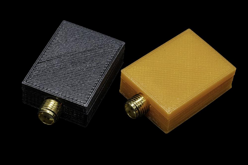
Mr. Frédéric Geissbuhler, CEO of Zero EC SA, added that “We searched for a place that can manufacture a micron scale Si prototype according to our design. Owing to their modernly equipped FAB and very talented team, they reached this incredible achievement. Dr. Abulafia proved that the Bar-Ilan Nano center is one of the best places to collaborate with. They were able to produce a prototype demonstrating a channel density of 5 microns, 1M channels on 1cm x 1cm silicon chip. This technology has the potential to resolve existing bottlenecks for data transport in various applications, but it also can become a real competition in almost all applications for fiber optics or copper in the future”.
About Bar-Ilan nano center (Bar Ilan Institute of Nanotechnology and Advanced Materials)
Established in 2007 BINA boasts 68 cutting-edge laboratories as well as state-of-the art „Scientific Service“.
Also providing tailored services to enterprises in a variety of domains such as CPM, nanofabrication, surface analysis, Bar-Ilan university never ceases to reinvent itself since its creation. Its evolution is exemplary.
BINA’s remarkable productivity – in publications, grants, patents, and in the creation of successful start-ups from basic science breakthroughs – have made BINA highly sought after as an R&D partner. In addition to academic collaborations with some of the world’s top research institutes, BINA currently partners with leading multi-national corporations.
The company was founded in Switzerland in 2011. With additional sites in Israel and Germany and a team of highly decorated scientists, Zero EC collaborates with leading international institutes and universities (including Fraunhofer, Bar-Ilan University, Weizmann Institute of Science, Humboldt University of Berlin, and many more). Its total financing to date is in the double-digit million euro range.
Zero EC SA
Le Château 3
CH2028 Vaumarcus
Telefon: 01705291257
http://www.0ec.com
Head of Business Development
E-Mail: info@zeroec.ch
![]()